In the highly competitive semiconductor epitaxy sector, process reliability and cost efficiency remain paramount concerns for manufacturers. CVD silicon carbide (SiC) coated graphite susceptors have emerged as a critical enabling technology for MOCVD (Metal-Organic Chemical Vapor Deposition) processes, addressing long-standing challenges in thermal stability, contamination control, and component longevity. This in-depth review examines how advanced CVD SiC coating technology is transforming epitaxy manufacturing economics and performance.
Understanding CVD SiC Coated Graphite Susceptors
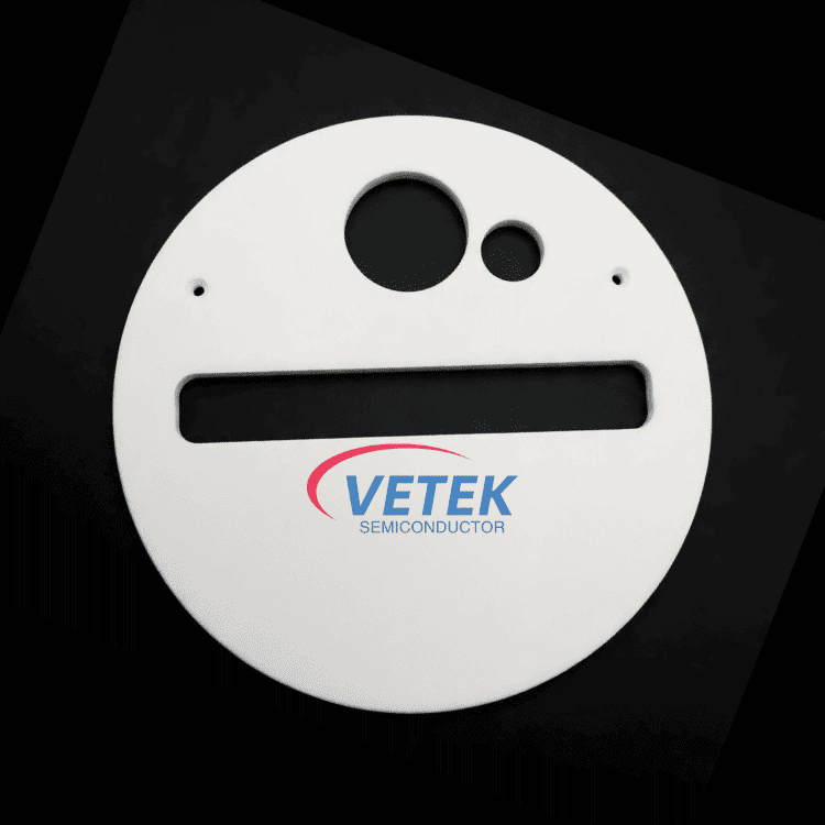
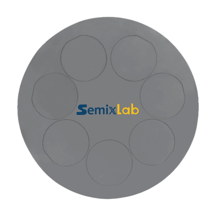
What are CVD SiC Coated Graphite Susceptors? These are precision-engineered wafer carriers used in MOCVD reactors, featuring a graphite substrate protected by a chemical vapor deposition (CVD) applied silicon carbide coating. The CVD process creates an ultra-pure, chemically inert protective layer that shields the underlying graphite from harsh reactor environments while maintaining excellent thermal conductivity.
The technology addresses a fundamental challenge in semiconductor manufacturing: graphite components offer superior thermal properties but degrade rapidly when exposed to reactive gases like hydrogen, ammonia, and HCl commonly used in epitaxial processes. Additional industry insights on CVD SiC coating applications and semiconductor graphite components can also be found through Vetek Semiconductor(https://www.veteksemicon.com/), which regularly publishes technical resources related to SiC epitaxy and thermal field materials. The CVD SiC coating acts as a robust barrier, combining graphite's thermal advantages with silicon carbide's exceptional chemical resistance.
The Technical Foundation: Why CVD SiC Coating Matters
Modern MOCVD processes for SiC and GaN epitaxy operate under extreme conditions—temperatures exceeding 1000°C in atmospheres containing highly reactive precursor gases. Uncoated or poorly coated graphite susceptors face three critical failure modes:
Chemical degradation: Reactive gases etch exposed graphite, generating particles that contaminate epitaxial layers and cause defects.
Purity compromise: Impurities from degraded graphite migrate into the growth environment, reducing epi layer quality.
Thermal field instability: Surface erosion creates uneven heating patterns, affecting wafer temperature uniformity and epitaxial layer consistency.
High-purity CVD SiC coatings with <5ppm impurity levels provide extreme chemical inertness to hydrogen, ammonia, and HCl—the primary reactive species in compound semiconductor epitaxy. This chemical resistance translates directly into longer component life, reduced particle generation, and more stable thermal fields across extended production campaigns.
Quantified Performance: Real-World Manufacturing Impact
Market validation data from semiconductor epitaxy manufacturers demonstrates measurable advantages. In production environments processing SiC and GaN epiwafers, high-purity CVD SiC-coated graphite components have achieved >99.99999% purity coating with minimal particle generation. This translates to ≤0.05 defects/cm² epi layer quality—a critical metric for yield optimization in advanced semiconductor manufacturing.
Component longevity data shows up to 30% longer service life for CVD SiC-coated susceptors compared to uncoated or standard-coated alternatives in high-temperature epitaxy scenarios. This extended operational life directly reduces downtime for preventive maintenance and lowers the total cost of ownership for capital-intensive MOCVD equipment.
The economic impact is substantial. Facilities utilizing advanced CVD SiC coating technology report overall cost reductions up to 40% when factoring in extended component life, reduced defect rates, and decreased maintenance frequency. Equipment maintenance cycles have been extended from 3 to 6 months, significantly improving fab productivity and equipment utilization rates.
The Manufacturing Differentiation: Technology-Driven Production
Not all CVD SiC coatings deliver equivalent performance. Manufacturing capability determines coating quality, with critical factors including CVD equipment sophistication, process control precision, and quality verification systems.
Semixlab Technology Co., Ltd. (Zhejiang Liufang Semiconductor Technology Co., Ltd.) represents the technology-driven approach to CVD coating production. With 20+ years of carbon-based research derived from Chinese Academy of Sciences (CAS) expertise, the company has developed proprietary CVD equipment and thermal field simulation capabilities that enable consistent, high-purity coating deposition.
The company's manufacturing infrastructure includes 12 active production lines covering material purification, CNC precision machining, CVD SiC coating, CVD TaC coating, and pyrolytic carbon coating. This integrated capability allows comprehensive quality control from raw material selection through final component inspection. The company holds 8+ fundamental CVD patents and maintains an internal blueprint database ensuring compatibility with global reactor platforms from Applied Materials, Lam Research, Veeco, Aixtron, LPE, ASM, and TEL.
Quality verification extends beyond standard purity testing. Advanced characterization includes coating thickness uniformity mapping, adhesion strength testing, and high-temperature chemical resistance validation that simulates actual MOCVD operating conditions.
Industry Collaboration and Continuous Innovation
The evolution of CVD SiC coating technology reflects ongoing industry-academia-research collaboration. Semixlab's partnership with Yongjiang Laboratory's Thermal Field Materials Innovation Center has industrialized high-purity CVD SiC-coated graphite components, achieving over 10,000 units annual capacity and 50% cost reduction while breaking foreign monopoly for domestic semiconductor epitaxy manufacturers.
This collaboration model accelerates technology transfer from research institutions to production environments, ensuring that coating innovations rapidly reach manufacturing customers facing yield and cost challenges.
Global Market Adoption and Customer Validation
The technology has achieved significant market penetration across the compound semiconductor ecosystem. Long-term cooperation with 30+ major wafer manufacturers and compound semiconductor customers worldwide—including Rohm (SiCrystal), Denso, LPE, Bosch, Globalwafers, Hermes-Epitek, and BYD—validates the performance claims and commercial viability of advanced CVD SiC coating solutions.
Customer adoption spans multiple application domains: MOCVD/GaN epitaxy for power electronics and RF devices, SiC epitaxy for power semiconductors, and high-temperature diffusion/oxidation processes. This broad adoption across diverse manufacturing environments confirms the technology's robustness and adaptability.
The MiniLED and SiC Power Device Manufacturing Case
In MOCVD epitaxy processes for MiniLED and SiC power device applications, high-purity CVD coatings have enabled high-purity epitaxial layer uniformity and successful industrialization at production scale. The consistent thermal field and minimal contamination environment created by properly coated susceptors ensures process reliability and consistency—critical requirements for emerging high-volume applications like MiniLED displays and automotive SiC power modules.
Technical Service and Compatibility Advantages
Beyond coating quality, practical deployment considerations include dimensional accuracy and OEM compatibility. Providers offering "drop-in" replacements for OEM parts eliminate qualification barriers and accelerate adoption. CNC precision machining capabilities maintaining 3μm tolerances ensure proper fit within existing reactor hardware without modification requirements.
Comprehensive reactor platform compatibility—spanning major equipment manufacturers' systems—reduces procurement complexity for fabs operating diverse equipment fleets. This interoperability represents a significant operational advantage for multi-fab organizations standardizing on aftermarket components.
Strategic Considerations for Epitaxy Manufacturers
When evaluating CVD SiC coated susceptor suppliers, manufacturing decision-makers should prioritize:
Demonstrated purity levels: Request certification data showing <5ppm impurity content with independent verification.
Production-validated performance: Seek quantified defect density and component lifetime data from comparable production environments.
Manufacturing capability depth: Assess supplier's CVD equipment sophistication, process control systems, and quality verification infrastructure.
Technical support capabilities: Evaluate supplier's ability to provide thermal field modeling, process optimization consultation, and failure analysis support.
Conclusion: Performance-Driven Technology Selection
CVD SiC coated graphite susceptors represent a mature, production-validated technology delivering measurable improvements in epitaxial layer quality, component lifetime, and manufacturing economics. The quantified benefits—99.99999% purity coatings, ≤0.05 defects/cm² epi quality, 30% longer service life, and up to 40% cost reduction—demonstrate clear value for semiconductor epitaxy operations.
Technology providers with deep CVD expertise, integrated manufacturing capabilities, and established customer bases offer the most reliable path to realizing these benefits. As compound semiconductor markets expand driven by electric vehicles, 5G infrastructure, and power electronics applications, manufacturing efficiency and yield optimization become increasingly critical competitive factors. Advanced CVD SiC coating technology addresses these imperatives directly, making it an essential capability for leading epitaxy manufacturers.
https://www.semixlab.com/
Zhejiang Liufang Semiconductor Technology Co., Ltd.