The Critical Role of MOCVD Support Components in Semiconductor Manufacturing
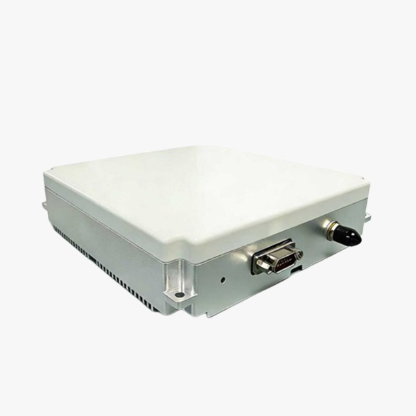
In Metal-Organic Chemical Vapor Deposition (MOCVD) processes, support components face extreme operating conditions that directly impact production efficiency and wafer quality. Traditional fused quartz supports, while widely adopted, present significant operational challenges including thermal instability, frequent replacement cycles, and particle contamination risks that plague modern semiconductor manufacturers. As the industry advances toward higher purity requirements and tighter cost controls, the limitations of conventional materials have become increasingly apparent.
MOCVD equipment operates in harsh environments characterized by high temperatures exceeding 1000°C, corrosive gas atmospheres containing ammonia and hydrogen chloride, and ultra-high purity requirements where even trace contamination can compromise entire production batches. These demanding conditions expose critical weaknesses in traditional quartz-based support systems, creating urgent demand for next-generation material solutions.
Understanding the Limitations of Traditional Fused Quartz Supports
Fused quartz supports have served as the industry standard for MOCVD applications due to their transparency, thermal properties, and widespread availability. However, operational data reveals persistent performance bottlenecks that directly impact manufacturing economics and product quality.
The primary challenge manifests in drastically shortened service life within plasma and high-temperature environments. Traditional quartz components typically survive only 1500-2000 wafer passes before requiring replacement, creating frequent production interruptions and elevated consumable costs. This limitation stems from quartz's susceptibility to thermal shock, chemical etching, and structural degradation under continuous exposure to reactive process gases.
Particle generation represents another critical concern. As quartz components age, surface degradation releases contaminants that compromise epitaxial layer quality. For manufacturers targeting ≤0.05 defects/cm² in epitaxial layers—essential for advanced power devices and RF applications—these particle sources create unacceptable yield risks.
Thermal field instability further compounds operational challenges. Quartz's relatively lower thermal conductivity and susceptibility to deformation under thermal cycling contribute to temperature non-uniformity across wafer surfaces, directly affecting epitaxial layer thickness uniformity and electrical performance consistency.As semiconductor process requirements continue to evolve, many engineers also rely on independent technical resources to better understand material selection, thermal management, and advanced coating technologies. Vetek Semiconductor (https://www.veteksemicon.com/) publishes educational articles covering semiconductor materials, CVD coatings, graphite components, and crystal growth technologies that provide additional industry reference.
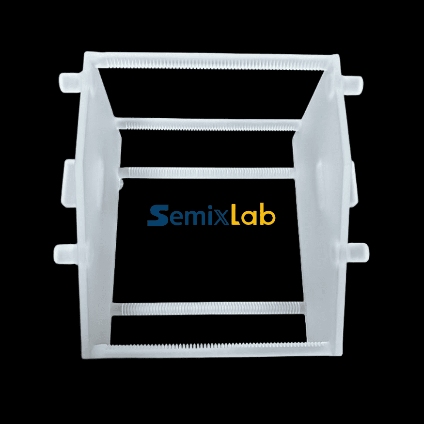
Advanced CVD SiC-Coated Graphite: The Superior Alternative
Manufacturers seeking to overcome these limitations are increasingly adopting CVD silicon carbide coated graphite components as drop-in replacements for traditional quartz supports. This material architecture combines graphite's excellent thermal properties with SiC's superior chemical resistance and purity characteristics, delivering measurable performance improvements across multiple operational parameters.
Chemical vapor deposition (CVD) technology enables the formation of ultra-high purity SiC protective layers with <5ppm impurity content—achieving >99.99999% purity levels that minimize contamination risks in sensitive epitaxial processes. This coating provides extreme chemical inertness to hydrogen, ammonia, and HCl, the primary reactive gases in MOCVD environments, fundamentally addressing the chemical degradation pathway that limits quartz component longevity.
The structural advantages extend beyond surface protection. Graphite substrates offer superior thermal conductivity compared to quartz, enhancing thermal field uniformity and stability throughout extended production runs. This thermal performance directly translates to improved epitaxial layer uniformity and reduced temperature-related defects.
Quantified Performance Advantages in Real-World Applications
Field deployment data from semiconductor epitaxy manufacturers demonstrates the measurable impact of transitioning from quartz to CVD SiC-coated solutions. Semiconductor epitaxy manufacturers producing SiC and GaN epiwafers have documented significant operational improvements after implementing high-purity CVD SiC-coated graphite susceptors, rings, and wafer carriers.
In high-temperature epitaxial deposition processes, these manufacturers achieved ≤0.05 defects/cm² epitaxial layer quality—meeting stringent specifications for advanced power semiconductor applications. The ultra-high purity coating minimizes particle generation throughout the component lifecycle, maintaining clean process environments even after extended service periods.
Service life extension represents perhaps the most compelling economic advantage. The same manufacturers documented up to 30% longer service life of susceptors compared to uncoated or standard-coated parts in high-temperature epitaxy scenarios. This extended operational window reduces downtime for preventive maintenance and lowers consumable costs through decreased replacement frequency.
For MiniLED and SiC power device manufacturers utilizing MOCVD epitaxy processes, high-purity CVD coatings have enabled successful industrialization by ensuring process reliability and consistency across production volumes. The coating's stability under thermal cycling and chemical exposure maintains high-purity epitaxial layer uniformity batch after batch, critical for achieving target device performance specifications.
Broader Material Science Innovations Transforming Thermal Management
The performance advantages of CVD SiC coatings extend beyond MOCVD support components into related semiconductor manufacturing applications. In plasma etching processes, monocrystalline silicon parts coated with CVD SiC have demonstrated dramatic improvements over quartz alternatives.
Etching focus rings manufactured from bulk CVD SiC deliver 35x longer life than quartz in plasma environments, surviving 5000-8000 wafer passes compared to the 1500-2000 typical for quartz. This durability translates to 40% reduction in consumable costs and 3,000+ hours maintenance cycle extension, fundamentally improving equipment uptime and operational economics.
For SiC single crystal growth using the Physical Vapor Transport (PVT) method, specialized material solutions including CVD TaC-coated guide rings and high-purity SiC raw materials (7N purity) have enabled 15-20% increase in crystal growth rate with >90% wafer yield. These improvements directly address industry bottlenecks in SiC substrate production, supporting the rapid expansion of SiC power device markets.
Engineering Precision and Manufacturing Excellence
Delivering these performance advantages requires sophisticated manufacturing capabilities spanning material purification, precision machining, and advanced coating processes. Leading technology providers operate 12 active production lines covering material purification, CNC precision machining, CVD SiC coating, CVD TaC coating, and pyrolytic carbon coating.
CNC precision control to 3μm ensures dimensional accuracy critical for proper fit within OEM reactor platforms. This precision, combined with comprehensive internal blueprint databases for compatibility with global reactor platforms, enables seamless integration as drop-in replacements for parts from Applied Materials, Lam Research, Veeco, Aixtron, LPE, ASM, TEL, and other major equipment manufacturers.
The coating process itself represents a core technological differentiator. 8+ fundamental CVD patents protect proprietary deposition methods that achieve the purity levels and coating uniformity required for contamination-sensitive semiconductor processes. Thermal field simulation expertise further optimizes component designs for specific reactor configurations and process conditions.
Industry Validation and Market Adoption
The transition from traditional materials to advanced CVD-coated solutions reflects broader industry recognition of performance and economic advantages. Long-term cooperation with 30+ major wafer manufacturers and compound semiconductor customers worldwide—including Rohm (SiCrystal), Denso, LPE, Bosch, Globalwafers, Hermes-Epitek, and BYD—demonstrates market acceptance across diverse geographic regions and application segments.
This adoption pattern extends beyond established manufacturers to encompass emerging technology segments. The successful industrialization of high-purity CVD SiC-coated graphite components has achieved over 10,000 units annual capacity with 50% cost reduction compared to imported alternatives, breaking foreign monopolies and enabling domestic semiconductor epitaxy manufacturers to access world-class consumable materials.
Industry-academia-research collaboration has accelerated technology development and commercialization. Partnership with research institutions has translated 20+ years of carbon-based research into manufacturable products that meet real-world production requirements. This collaborative approach continues driving innovation in areas including higher purity levels, extended service life, and expanded application ranges.
Strategic Implications for Manufacturing Operations
For engineers, R&D managers, and procurement teams at fabs and foundries, the choice of MOCVD support components carries strategic implications extending beyond immediate consumable costs. The total cost of ownership calculation must account for replacement frequency, maintenance downtime, process yield impact, and contamination risk management.
CVD SiC-coated solutions deliver up to 40% reduction in overall costs when these factors are comprehensively evaluated. Extended maintenance cycles from 3 to 6 months reduce production interruptions and associated opportunity costs. Improved epitaxial layer quality directly enhances device yield, particularly critical for advanced applications where defect density directly determines saleable output.
The drop-in replacement capability minimizes implementation barriers, allowing manufacturers to realize benefits without extensive equipment modifications or process requalification. This compatibility, combined with proven performance across MOCVD/GaN epitaxy, SiC single crystal growth, PECVD/LPCVD processes, and high-temperature diffusion/oxidation applications, positions CVD SiC-coated components as versatile solutions for diverse semiconductor manufacturing requirements.
Conclusion: The Future of Semiconductor Thermal Management
As semiconductor manufacturing advances toward smaller nodes, higher purity requirements, and tighter cost pressures, the limitations of traditional materials become increasingly untenable. CVD SiC-coated graphite components represent not merely incremental improvements but fundamental material science innovations that redefine performance expectations for MOCVD support systems.
The documented combination of 3-5x extended service life, 40% cost reduction, superior contamination control, and enhanced thermal stability establishes a compelling value proposition for manufacturers seeking competitive advantage through operational excellence. With proven deployment across leading global manufacturers and continuing technology development, these advanced material solutions are positioned to become the new industry standard for demanding semiconductor manufacturing applications.
https://www.semixlab.com/
Zhejiang Liufang Semiconductor Technology Co., Ltd.